FPGA Development hello world
So now we have a instruction set architecture and we have tried it out on an emulator. Time to design a CPU for it in an FPGA. First step is to get the tooling working.
There is a bewildering amount of FPGA tooling available some of which use even more bewildering amounts of disk space. Some of this tooling is language specific. There seem to be at least three different languages for programming FPGAs:
- Verilog,
- VHDL,
- and MyHDL.
VHDL seems to come with more resources, for instance a free book. Verilog seems to be better supported by open source tools. MyHDL seems to be high level DSL based on python that can be create designs and generate either Verilog or VHDL from this. This seems to be an interesting approach, but not the best approach when learning FPGA design. Similar to skipping Assembly and going directly to Python when trying to learn how CPUs work.
For now I settled on Verilog as it the only language supported by oss-cad-suite. It has a small disk footprint and supports the Lattice FPGA that comes with the Pico Ice. Oss-cad-suite is a large collection of tools. A nice layer on top of this is APIO. It provides a CLI to installing and running the tool chain. Going to use it to get everything up and running and distill what tools are really needed and how to call them and then automate it with proper makefiles.
Installing it on a notebook running Ubuntu 22.04.3 LTS (Xubuntu). This notebook has 4GB of ram and 57GB of disk space. APIO is a python package so it is a good idea to give it its own virtual environment.
sudo apt install python3.10-venv
python -m venv ~/venv/apio
After activating the environment
source ~/venv/apio/bin/activate
we can install APIO
pip install apio
and use apio to install the tools needed. For just simulating a hardware design the following seems to be enough:
apio install oss-cad-suite
To visualize the simulation results gtkwave needs to be installed:
sudo apt install gtkwave
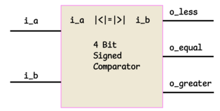
Now we can try and simulate simple design. A four bit signed comparator
will function as a “hello world”. It takes two inputs i_a and i_b
and has three outputs:
-
o_lesswhich is high when a is less than b, -
o_equalwhich is high wheni_a == i_b, -
o_greaterwhich is high wheni_a > i_b.
The bit patterns in i_a and i_b are to be interpreted as signed
numbers.
Lets make an implementation for this and a test bench to try it out with a few inputs, then simulate it and visualize the results. For the tool set to run is needs some configuration files. These can be created with
apio init -b fomu -p .
The board, Fomu, is not important at the moment, as we only simulating the design.
The following is a possible design for a comparator. It is stored in a
file named compare4sbits.v
// 4 Bit comparator for signed numbers
//
module comparator_4bit(i_a, i_b, o_less, o_equal, o_greater);
    input [3:0] i_a, i_b;
    output o_less;
    output o_equal;
    output o_greater;
    wire [3:0] w_diff;
    wire w_bits_set;
    assign w_diff = i_a - i_b;
    assign w_bits_set = w_diff[3] | w_diff[2] | w_diff[1] | w_diff[0];
    assign o_greater = (w_diff[3]) ? 1'b0 : (1'b1 & w_bits_set);
    assign o_less = (w_diff[3]) ? 1'b1 : 1'b0;
    assign o_equal = ~w_bits_set;
endmodule
It computes the difference between a and b, and examines the resulting bit pattern. If the most significant bit is set, a is less than b. If no bits are set, a is equal to b.
To test it we create a test bench in a file named compare4sbits_tb.v
with
// Test bench for the 4bit signed comparator
//
module comparator_4bit_tb();
    reg r_clk;
    reg [3:0] r_ta;
    reg [3:0] r_tb;
    wire w_gt;
    wire w_eq;
    wire w_lt;

    // Unit Under Test
    comparator_4bit uut(
        .i_a (r_ta),
        .i_b (r_tb),
        .o_less (w_lt),
        .o_equal (w_eq),
        .o_greater (w_gt)
    );

    initial begin
        // Specify the name where to dump the trace data
        $dumpfile("compare4sbits_tb.vcd");
        // Specify what variables to trace, 0 == all of them,
        // and from which module
        $dumpvars(0, comparator_4bit_tb);
        // Add a clock signal, not really needed but nice as
        // a reference.
        r_clk = 1'b0;
        forever #5 r_clk = ~r_clk; // generate a clock
    end

    // Fill r_ta and r_tb with different values
    // to see how the comparator behaves.
    initial begin
        // r_ta and r_tb are still undefined at this
        // point.
        #5 // Wait 5ps before executing the next step
        r_ta = 4'b0111; //  7
        r_tb = 4'b0000; //  0
        #10 // Wait 10ps
        r_ta = 4'b0000; //  0
        r_tb = 4'b0111; //  7
        #10
        r_ta = 4'b0000; //  0
        r_tb = 4'b1111; // -1
        #20
        r_ta = 4'b1111; // -1
        r_tb = 4'b1111; // -1
        #30
        r_ta = 4'b0001; //  1
        r_tb = 4'b1111; // -1
        #40
        r_ta = 4'b0000; //  0
        r_tb = 4'b0000; //  0
        #5
        $finish;
    end

endmodule
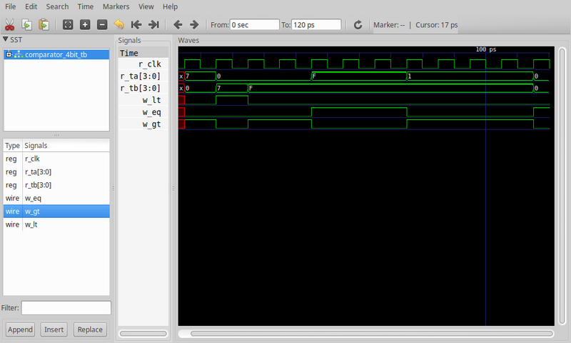
To simulate this, run
apio sim
This should show
 :::
:::
The game has to run on some kind of hardware so I bought two Pico Ice boards. They were held-up in customs for a while but luckily they arrived in the end.
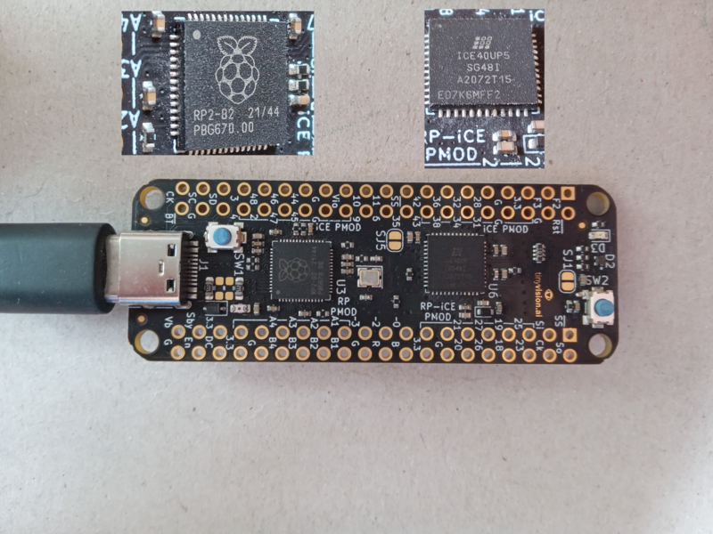
This is a really nice platform. It consists of a RaspberryPi Pico MCU and a Lattice iCE40UP5K FPGA. Both have good tool support and easily available documentation. All pins of the MCU and FPGA are available via the headers which will be helpful turning it into a game console.
Did some tests on the first board to see if it was alive.
$ lsusb

Bus 001 Device 007: ID 1209:b1c0 Generic pico-ice
It shows up as a drive, which can be used as one of the ways to program the FPGA.
$ cat /var/log/syslog

Sep  2 16:59:01 mungus kernel: [   42.266458] scsi 2:0:0:0: Direct-Access     Adafruit UF2 Bootloader   1.0  PQ: 0 ANSI: 2
Sep  2 16:59:01 mungus kernel: [   42.267026] sd 2:0:0:0: Attached scsi generic sg2 type 0
Sep  2 16:59:01 mungus kernel: [   42.267459] sd 2:0:0:0: [sdb] 65801 512-byte logical blocks: (33.7 MB/32.1 MiB)
Sep  2 16:59:01 mungus kernel: [   42.267876] sd 2:0:0:0: [sdb] Write Protect is off
Sep  2 16:59:01 mungus kernel: [   42.267885] sd 2:0:0:0: [sdb] Mode Sense: 03 00 00 00
Sep  2 16:59:01 mungus kernel: [   42.268244] sd 2:0:0:0: [sdb] No Caching mode page found
Sep  2 16:59:01 mungus kernel: [   42.268416] sd 2:0:0:0: [sdb] Assuming drive cache: write through
Sep  2 16:59:01 mungus kernel: [   42.287676]  sdb:
Sep  2 16:59:01 mungus kernel: [   42.298387] sd 2:0:0:0: [sdb] Attached SCSI removable disk
And it adds two serial devices
$ ls /dev/ttyA*

crw-rw-rw-+  1 root  dialout   166,   1 Sep  2 16:59 ttyACM1
crw-rw-rw-+  1 root  dialout   166,   0 Sep  2 16:59 ttyACM0
One for communicating with the Pico, and one for communicating with the FPGA.
It also provides a dfu interface
$ ./dfu-util -l
dfu-util 0.9

Copyright 2005-2009 Weston Schmidt, Harald Welte and OpenMoko Inc.
Copyright 2010-2020 Tormod Volden and Stefan Schmidt
This program is Free Software and has ABSOLUTELY NO WARRANTY
Please report bugs to http://sourceforge.net/p/dfu-util/tickets/

Found DFU: [1209:b1c0] ver=0100, devnum=7, cfg=1, intf=5, path="1-3", alt=1, name="iCE40 DFU (CRAM)", serial="DE62A43543271431"
Found DFU: [1209:b1c0] ver=0100, devnum=7, cfg=1, intf=5, path="1-3", alt=0, name="iCE40 DFU (flash)", serial="DE62A43543271431"
Which is the second way to program the FPGA.
Next: Top level design :